


- A photomask is tool used for productions of components including electronic devices (semiconductors), displays, PCB, MEMS. It is a master copy for the patterning.
- Photolithography is used to form PCB circuits and display patterns. Photomasks are used to transfer the patterns on the baseplates.
- A photomask acts just like "negative film" in photography, and that makes the baseplates "printing paper".

- Electronic devices - CPU, memories (semiconductor/ IC)
- Discreet components with a single task - transistors, memories
- Light receiving/ emitting elements - CCD/CMOS image sensors, LED
- PWB - motherboards
- Display devices - LCD, OLED
- MEMS(Micro Electro Mechanical System) - acceleration sensors
- Magnetic heads for hard disks
- Heads for inkjet printers

A reticle is usually used in the front-end process of semiconductor fabrication.
A pattern to be transferred to silicon wafers is produced by chrome etching on a glass plate. The pattern is transferred to wafers through an exposure device.
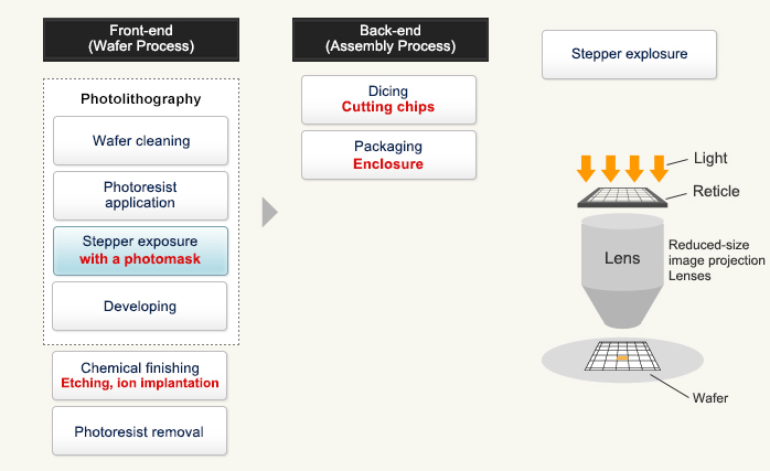
- Front-end process is a process to form circuits on wafers to be made into semiconductors.Reticles are used for prior processing for the exposure process.
- Back-end processing is an assembly process that includes dicing (cutting the wafer into chips) and packaging (protection) after forming the circuits.
- A stepper is an exposure device used for semiconductor fabrication. It transfers a design on the reticle to wafers by light with wavelength matching the circuit line width.